¶ I2S and SPI Signal Quality
This page documents some signal quality measurements that I performed on FluidNC controller boards.
¶ Introduction
FluidNC controllers typically have an SPI bus that talks to the SD Card and sometimes to TMC stepper drivers, and an I2S bus that drives shift registers for stepper drivers. Both buses have a clock signal and one or more data signals. For reliable operation, one must ensure that the clock and data signals have good characteristics, with reasonably fast edges and minimal “ringing” (overshoot and undershoot). Those two considerations work against each other - faster edges are more prone to ringing.
There are two main factors that affect these characteristics - layout and termination.
- Good layout requires a linear trace without stubs or tee branches, driven from one end. It also requires a ground return path that closely follows the outgoing signal path. The faster the signal, the more that good layout is necessary. If the layout is bad, the signal will be more prone to ringing and to interference from nearby signals.
- Ringing can be minimized by resistive termination that matches the driving impedance to the inherent impedance of the signal trace in conjunction with its ground return path. There are different termination methods that are appropriate for different buses; for the signals that we are concerned with, series termination is often best. Series termination places a small value resistor - in the range of, say, 33 to 47 ohms - in series with the signal trace, located near the pin that drives the signal.
Signal quality is not directly affected by clock frequency; the edges (transitions between high and low) are what matters. However, bad signal quality can, in some cases, limit the frequency at which chips can function correctly. If the edges are too slow, one transition might not finish before the next one begins. Too much ringing can cause false clocking even at low clock frequencies.
¶ Drive Strength
MCU IO pins often have the ability to set the “drive strength”, controlling the amount of instantaneous current the GPIO can supply. This is effectively the same as a series termination resistor. If the drive strength is at its maximum value, it is as if there is a very low value series termination resistor. Conversely, if the drive strength is at its minimum value, it is like a higher value series termination resistor. ESP32 GPIOs have 4 drive strength settings: 0 for low, 1 for medium low, 2 for medium high, and 5 for high. The default, if you do not explicitly program the drive strength, is 2. Each IO pin's drive strength can be programmed individually.
FluidNC normally does not have a feature for setting drive strength, so all IO pins are at their default setting of 2 (medium high). For this exploration, I modified FluidNC to add the ability to configure the drive strength for any GPIO pin with attributes like :ds0, :ds1, :ds2, and :ds3.
¶ Measurement Methodology
I used a Siglent SDSD1102X dual-channel oscilloscope to observe various signals at different places. The scope has 100 MHz bandwidth at 1 GSa/s sample rate. The probes are rated at 100 MHz - but higher speed details can be observed with reduced amplitude.
For high speed signals, the probing method can influence the results, causing measurement errors due to the ground lead and other factors. To minimize such errors, I used a ground lead that was as short as feasible. I removed the probe's alligator clip ground lead and the tip shroud, leaving only the small probe tip with its ground ring. On that ground ring, I installed the small spiral spring accessory to provide a place to connect the ground. For each measurement point on the controller board, I tack-soldered two short 32 gauge wires, one on the signal and another on the nearest ground point. I wrapped the other end of the ground wire around the spiral spring and the other end of the signal wire around the probe tip. That resulted in a short, low capacitance, low inductance, small loop area probe attachment.
I repeated the measurements at different drive strength settings.
¶ Observations
¶ I2S Bus
The most sensitive I2S bus signals are BCK (clock) and DATA. BCK is routed to all of the shift register chips, while DATA goes directly only to the first chip in the chain, and subsequent chips are daisy-chained from the output of the preceding chip. The most critical data signal is the first one, since its trace is longest and thus most prone to ringing.
The controller board for the I2S measurements was a “FluidNC 6x CNC Controller v1.2”.
¶ I2S BCK and Data at the ESP32
This is with two probes attached to the I2S BCK and I2S data signals right at the ESP32 pins. The top (magenta) trace is data and the bottom (yellow) trace is BCK.
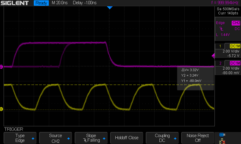
Note that the edges are somewhat faster.
This illustrates the first-order effects of changing the drive strength at the start of the trace, near the driver. But that is not the crucial point - the signal reception at the shift register is more important.
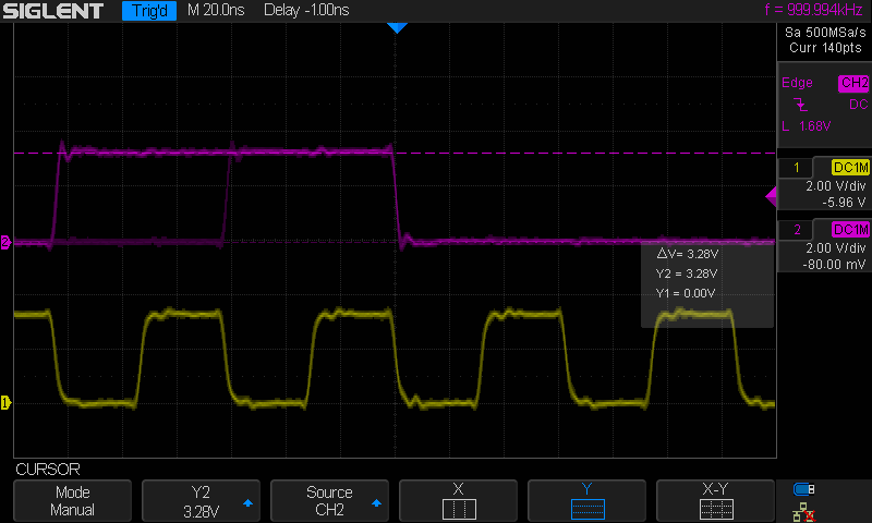
¶ I2S Data at the First Shift Register
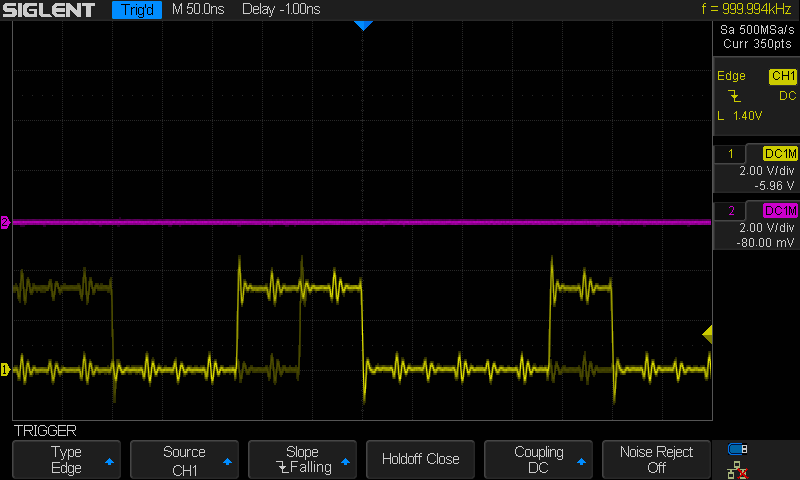
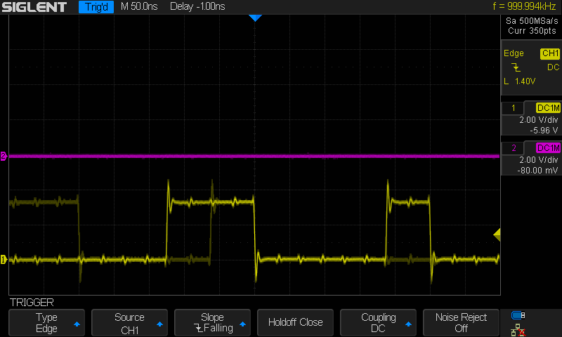
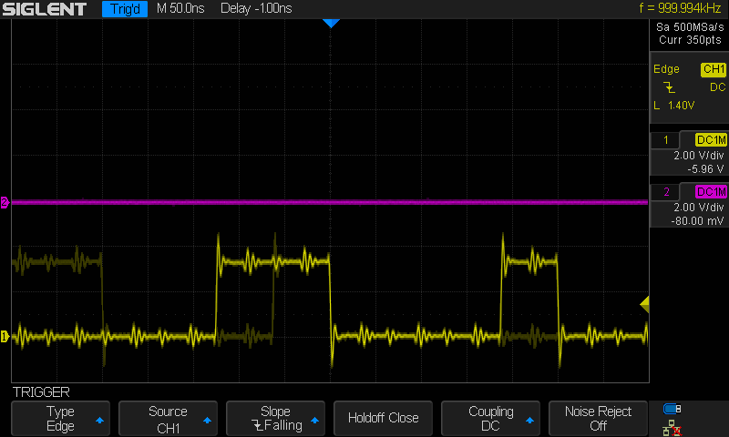
This next set of images shows the I2S Data signal probed at the input to the first shift register. The data signals at the other shift registers were not measured, because the daisy-chained traces are short and thus less susceptible to problems, and also because we have no control over the drive strength of the shift register data outputs. In these images, the second probe is not used so the top (magenta) trace is meaningless.
This first image shows the case where the Data drive strength and the BCK drive strength are both 3 (max). The ringing right after the low to high and high to low transitions is due to the data drive strength, basically reflections from the receiving end of the data signal line due to the mismatch between the high input impedance of the shift register chip and the inherent impedance of the signal trace. The periodic “bounces” between the transitions are interference from the BCK signal. Each BCK transition couples noise into the Data signal.
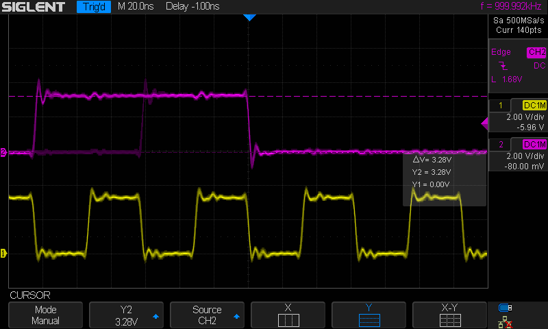
The interference between BCK and Data can be reduced by lowering the BCK drive strength to 1. Notice that the intermediate “bounces” are smaller. The data drive strength is still at 3, so the ringing after the transition edges is still pronounced.
The interference can be further reduced by lowering the BCK drive strength to 0, but the BCK edge rate at strength 0 is probably lower than ideal.

¶ Ground Plane Improvement
The layout of the 6x controller board has a small problem - the ground return path for the I2S BCK and Data signals “jogs” around a group of vertical traces on the bottom side of the board. This increases the “loop area” of the current path of the outgoing signal plus the ground return current, which can increase the susceptibility to interference from other signals, and can result in impedance discontinuities that can increase ringing. I wanted to see if improving this situation would significantly affect the signal quality. I scraped away the solder mask in various places on the ground plane and soldered on wires to create a return path that closely followed the routing of the I2S BCK and Data lines, thus reducing the loop area.
The signal appears almost identical to the “Data drive 3, clock drive 3” image above (with the ground plane unchanged). So, in this case, the suboptimal ground return path does not seem to be causing a measurable problem. The results were similar with different drive strengths - the ground change did not have much affect on the signal quality.
¶ SPI Bus
SPI has one clock line (SCK) and two data lines - MOSI (Master Out Slave In) from the ESP32 to the slave devices and MISO (Master In Slave Out) in the other direction, from slave device to the ESP32. SPI also has a separate CS- (Chip Select) line for each individual slave device.
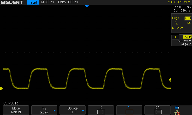
I initially measured the SPI signals on a “FluidNC 6x CNC Controller v1.2”, but the measurements were relatively uninteresting because that board connects the SPI bus only between the ESP32 and the adjacent SD Card. The traces are very short with a good ground plane underneath, so the signal quality was excellent. A more interesting case is a board that uses SPI for both an SD Card and also a collection of TMC drivers, leading to longer traces and more complex routing, with the possibility of resulting signal quality issues. So I measured the SPI bus signals on a “6-Pack CNC Controller V1p5”.
The board was populated with four TMC2130 SPI stepsticks, with the appropriate jumper setting for SPI driver configuration. The SPI SCK and MOSI signals were probed at the ESP32 pins using short jumper wires from the ESP32 socket to the probe tips and ground rings. The SD Card frequency was set to 8000000 Hz.


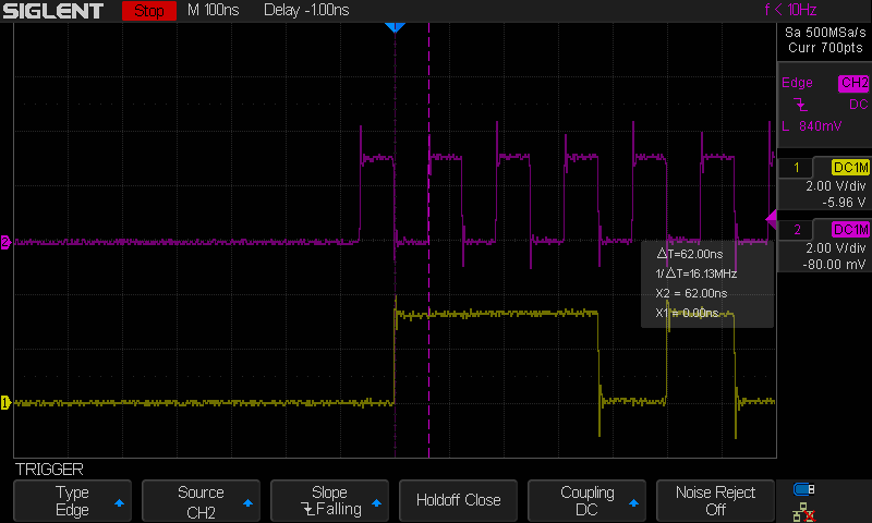
It appears that drive 1 is the best compromise between fast edges and little ringing.